Applied Materials Breakthrough To Bring OLED Displays to Tablets, PCs and TVs
21 11월 2024 - 9:30PM

Applied Materials, Inc. today introduced the MAX OLED™ solution, a
patented OLED pixel architecture and revolutionary display
manufacturing technology designed to bring the superior OLED
displays found in high-end smartphones to tablets, PCs and
eventually TVs.
OLED is the display technology of choice for the world’s leading
smartphone manufacturers because it offers superior display
quality, light and flexible form factors, and durability. However,
until today, it has proven challenging to scale OLED display
manufacturing to the larger glass panels used to make displays for
tablets, PCs and TVs.
Applied’s MAX OLED solution makes it easier to scale OLED
manufacturing from Gen 6* glass substrates to Gen 8* substrates,
which are approximately two times larger, and beyond. In addition,
the MAX OLED solution deposits OLED materials in a new way that
increases pixel brightness and resolution, reduces display energy
consumption, and lengthens display lifetime.
The MAX OLED solution has strong customer interest, with repeat
orders from multiple leading display manufacturers. Additionally,
Applied will supply a MAX OLED solution to Samsung Display, a
leading global manufacturer of OLED and QD-OLED panels. Samsung
Display will be bringing in an alpha system to assess this new
technology.
“The consumer electronics industry has been waiting for a
breakthrough that can bring OLED technology to the hundreds of
millions of tablets, PCs and TVs sold each year,” said Dr. Brian
Shieh, Group Vice President and General Manager of Applied’s
Display and Flexible Technology business. “We are proud to be
partnering with Samsung Display to help bring this revolutionary
technology to the global marketplace.”
Making OLED Displays Brighter, Longer-Lasting and More
Energy-Efficient
OLED displays are difficult to manufacture because the materials
used to emit red, green and blue are fragile and ruined by any
exposure to air or moisture. Applied’s MAX OLED solution is a
breakthrough technology that deposits and encapsulates each pixel
individually using a specially designed maskless process. Applied’s
approach is precise, fast and superior at maintaining the purity of
delicate OLED materials.
Applied’s proprietary solution uses selective deposition to
enable excellent pixel placement accuracy, more than doubling the
amount of OLED material per area as compared to previous
technologies. The technology can increase OLED display brightness
by as much as 3X and increase resolution by as much as 2.5X, to
approximately 2,000 pixels per square inch. The solution can also
reduce display power consumption by more than 30 percent and
increase display lifetime by up to 5X.
“Applied Materials has developed a true breakthrough in OLED
manufacturing technology that will enable better OLED displays at
more attractive prices,” said Ross Young, Co-founder and CEO of
Display Supply Chain Consultants (DSCC). “This technology has the
potential to accelerate OLED adoption in a range of markets, from
tablets and PCs to automobiles and micro-displays for AR/VR,
creating a catalyst for the entire display industry.”
New OLED Pixel Architecture, Process Recipe and
Integrated Materials Solution
The MAX OLED solution is more than equipment: it begins with a
proprietary pixel architecture built using a patented manufacturing
recipe that results in best-in-class OLED pixels and displays. The
manufacturing system combines a number of critical manufacturing
modules in a single, high-vacuum system that protects the delicate
OLED materials from the environment and reduces yield-killing
particles. The MAX OLED system integrates display glass handling,
multiple OLED deposition steps, and OLED encapsulation. Many of the
core technologies used by the MAX OLED solution have already been
proven by Applied in making large-area LCD screens at panel sizes
up to Gen 10.5*.
The MAX OLED solution reduces the energy consumption of OLED
display fabs, requires significantly less OLED materials, and
eliminates the need for mask cleaning chemicals, thereby reducing
the environmental impact of display manufacturing.
A Growing OLED Display Opportunity
Applied is already the world’s largest provider of display
manufacturing equipment, with a broad portfolio of products
spanning CVD** and PVD** deposition, CVD thin-film encapsulation,
and eBeam testing and inspection. The MAX OLED solution is expected
to more than double Applied’s served addressable market opportunity
in OLED display manufacturing.
*Gen 6 glass panel surface area = 2.78 square meters; Gen 8
surface area = 5.5 square meters; Gen 10 surface area = 9.9 square
meters**PVD = physical vapor deposition; CVD = chemical vapor
deposition
Forward-Looking StatementsThis press release
contains forward-looking statements, including those regarding
anticipated benefits of our new products and technologies, expected
growth and trends in our businesses and markets, industry outlooks
and demand drivers, technology transitions, and other statements
that are not historical facts. These statements and their
underlying assumptions are subject to risks and uncertainties and
are not guarantees of future performance. Factors that could cause
actual results to differ materially from those expressed or implied
by such statements include, without limitation: failure to realize
anticipated benefits of our new products and technologies; the
level of demand for semiconductors and for our products and
technologies; customers’ technology and capacity requirements; the
introduction of new and innovative technologies, and the timing of
technology transitions; market acceptance of existing and newly
developed products; the ability to obtain and protect intellectual
property rights in technologies; our ability to ensure compliance
with applicable law, rules and regulations; and other risks and
uncertainties described in our SEC filings, including our recent
Forms 10-Q and 8-K. All forward-looking statements are based on
management’s current estimates, projections and assumptions, and we
assume no obligation to update them.
About Applied MaterialsApplied Materials, Inc.
(Nasdaq: AMAT) is the leader in materials engineering solutions
used to produce virtually every new chip and advanced display in
the world. Our expertise in modifying materials at atomic levels
and on an industrial scale enables customers to transform
possibilities into reality. At Applied Materials, our innovations
make possible a better future. Learn more at
www.appliedmaterials.com.
Applied Materials Contact:Ricky Gradwohl
(editorial/media) 408.235.4676Liz Morali (financial community)
408.986.7977
A photo accompanying this announcement is available at
https://www.globenewswire.com/NewsRoom/AttachmentNg/8d0fc91b-33c4-41c3-9dca-3dcea6e988e2
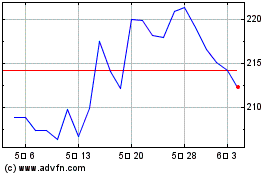
Applied Materials (NASDAQ:AMAT)
과거 데이터 주식 차트
부터 12월(12) 2024 으로 1월(1) 2025

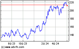
Applied Materials (NASDAQ:AMAT)
과거 데이터 주식 차트
부터 1월(1) 2024 으로 1월(1) 2025
